Currently, the development of key LED strip technology is the base material and wafer growth techniques. Sapphire substrate material in addition to traditional materials, silicon (Si), silicon carbide other than the (SiC), zinc oxide (ZnO), and gallium nitride (GaN), etc. are also the focus of current research. improving the efficiency of the LED chip LED lighting has become the key to enhance the overall technical indicators. In just a few years, with the chip structure, surface roughening, improving the design of multi-quantum well structure and a series of technology, LED luminous efficiency of major breakthroughs in the develo pment of LED chip structure shown in Figure 1. LED quantum efficiency will be further improved, the luminous efficiency of LED chips will also rise.
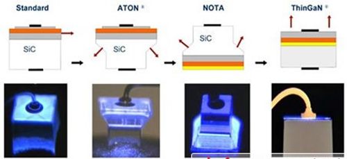
(Figure 1) The development course of LED chip structure
Thin film chip technology (Thinfilm) is the key technology to produce ultra-bright LED chips, can reduce the light loss, 97% of the light output from the front through the bottom of the reflecting surface
not only greatly improve the luminous efficiency of LED, also simple lens design.
Three packaging technology introduction
High-power LED packaging technology can be divided into a single chip, multi-chip integration and chip-board package three categories , the following will be described:
Luminous efficiency, heat dissipation and reliability advantages for single chip package Single-chip packaging technology package is the most widely used,its main technical bottleneck is the coating technology and fluorescent powder yield rate, chip color temperature,. Advantages of single-chip package is the high light efficiency, easy to disperse heat, easy to light distribution and reliability.Package shape and internal structure of SemiconductorsMulti chip integrated package for small volume can reach high luminous flux Multi-chip integrated high-power LED module assembly is currently the most common form of another package, can be divided into low-power and high-power chip integration of components into two categories,the former with six low-power chip integration of a 1watt high-power LED components,such integration led cod has the advantage of low cost is the main way to make a lot of high-power LED assembly.(Figure 2) by optimizing the design, the thermal resistance of the final product can be controlled 3.1 ℃ per watt, and can drive up to 15 watts of high power. The advantage of this package is to achieve a high flux in a very small space.
(Figure 2)
COB effectively improve defects — dissipation heat
COB technology follows the traditional semiconductor technology, which directly to the LED chip is fixed on the printed circuit board (PCB). Using this technique, there are only 0.3 mm thickness of less than LED.Because the LED chip in direct press close to the PCB board,increasing the area of heat conduction and heat dissipation problems can be improved. This package to form more small power chip. This package mostly low-power-led-chip